Printed Circuit Board
Written by Rachel Yan
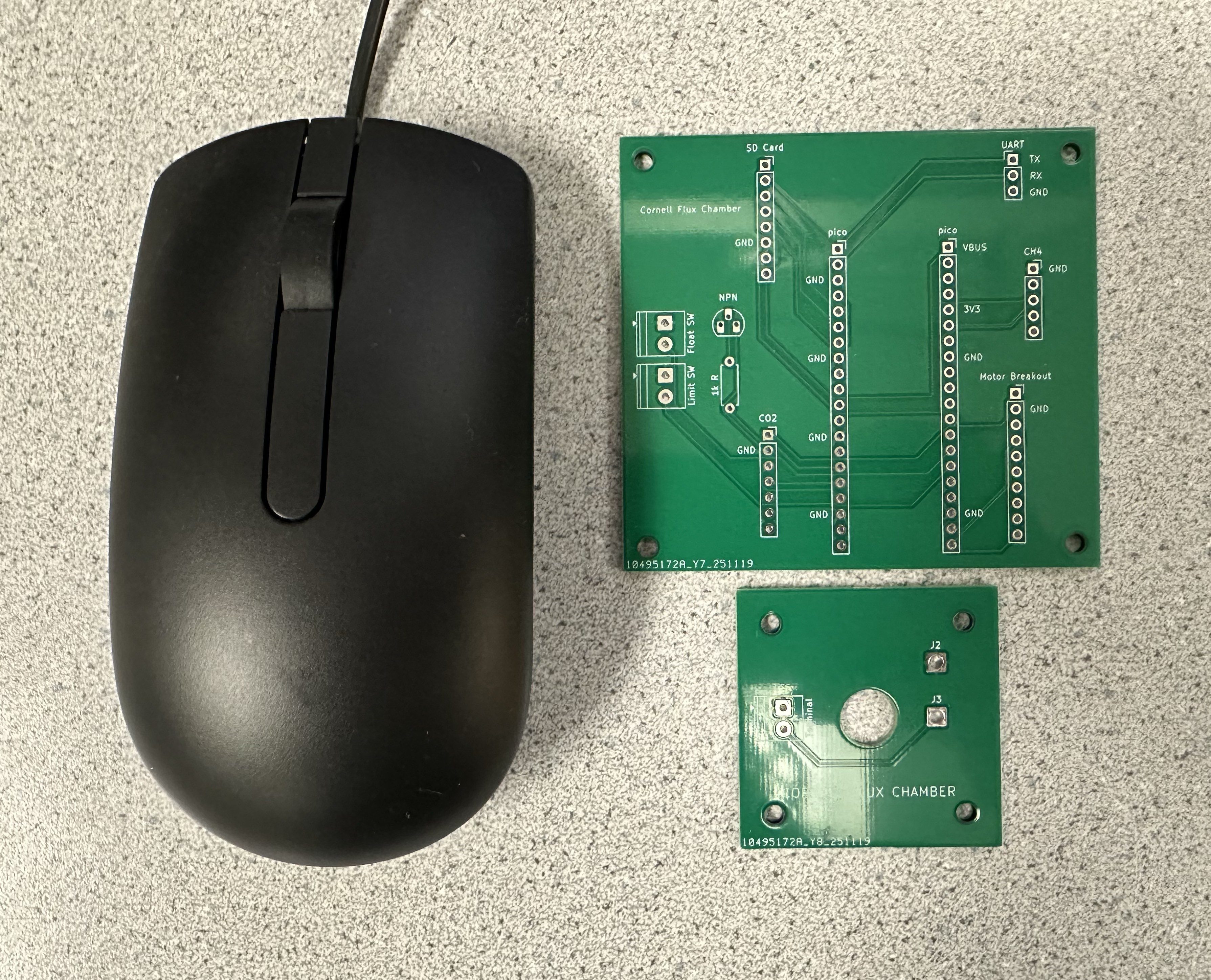
The printed circuit board (PCB) is designed to serve as a consolidation of the electonic devices wiring and power management board for the flux chamber system. It simplifies field assembly by putting all key connections, including CO₂ and methane sensors, motor drivers, SD card breakout, and the Pico into a compact, easily solderable board. The PCB includes mainly header sockets which allow quick replacement or testing of each component. There are also screw terminals to support the slightly longer wiring for the float switch and limit switch. To accommodate the mounting needs of the limit switch on the motor, we also created a seperate breakout PCB for only the limit switch. The PCBs makes the system's electronic system more convenient and reliable for building and testing.
The design files can be found in the CornellFluxChamber Github repository.
PCB Design
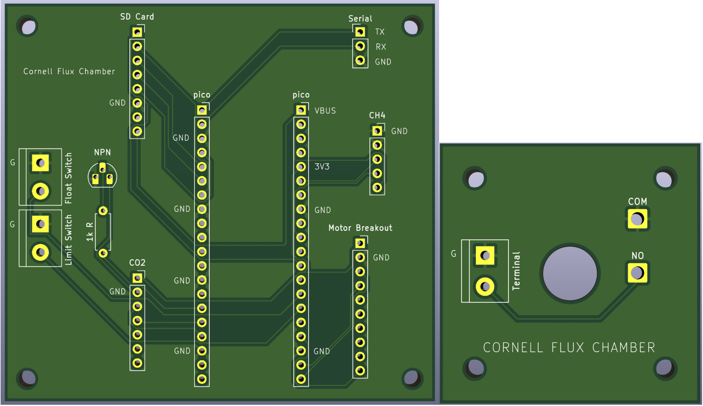
The PCB is designed using KiCAD and printed at JLCPCB. The main PCB is sized to be 77.11 mm x 71.33 mm, and the small PCB is sized to be 42.3 mm x 42.3 mm. The designs are as follows:
Supported Connections
The pin connections are the same as the wired versions (please check the other pages for wiring and pin information).
The main PCB includes labeled pin sockets or terminals for: | Label | Conenction Type | Description | | :------------: | :----------------: | :---------------------------------: | | pico | 2 * 1x20 Header | Raspberry Pi Pico Microcontroller | | Serial | 1x3 Header | Serial Communication Port | | CH4 | 1x5 Header | Methane Sensor | | Motor Breakout | 1x10 Header | Motor Driver Breakout Board | | SD Card | 1x8 Header | SD Card Breakout Board | | CO₂ | 1x7 Header | CO₂ Sensor | | NPN | Through hole | 2N3904 NPN Transistor | | 1k R | Through hole | 1kΩ Resistor | | Float Switch | 1x2 Screw Terminal | Float Switch Wires | | Limit Switch | 1x2 Screw Terminal | Limit Switch Wires |
The small breakout PCB includes labeled pin sockets or terminals for: | Label | Conenction Type | Description | | :------------: | :----------------: | :---------------------------------: | | Limit Switch | 1x2 Screw Terminal | Limit Switch Wires | | COM | Through hole | COM Side of Limit Switch | | NO | Through hole | NO Side of Limit Switch |
Main Layout Design
The PCB layout was designed with two main priorities: to fit within the limited space of the flux chamber and to support all key components with clear, reliable routing. Because we are using multiple sensors and breakout boards, careful placement and spacing was necessary to ensure both compactness and functionality.
We placed the Raspberry Pi Pico header as close to the bottom edge of the PCB as possible. This decision was made because the USB cable used to power the Pico has a rigid plug that sticks out from the top of the board. By positioning the Pico at the bottom, most of the USB connector remains within the footprint of the PCB, helping to protect the cable and reducing strain.
The four main breakout boards were positioned around the Pico based on their pin connections. The methane sensor and motor breakout board were placed to the right of the Pico, while the CO₂ sensor (SCD30) and SD card breakout were placed on the left. Since we use a full ground plane to keep all devices grounded together for electrical stability, routing had to be planned carefully to avoid creating isolated ground sections. This took some effort to adjust trace paths and header positions so that the ground plane could remain continuous.
Because all breakout boards are connected through pin headers, we also accounted for the physical shape and clearance of each module. For example, the methane sensor has metal pins that stick out from its left side, so we shifted its header slightly to the right to avoid contact with other parts. Similarly, the SD card breakout has its pins on the right edge, but it requires extra vertical space above and below for plugging and unplugging the card. We made sure to leave enough space around these components during placement.
Some components also have external interaction requirements. For example, the screw terminals must allow room for wire entry and tightening, and the SD card needs space for easy card access. To support this, we made sure both components are placed along the outer edge of the board, and oriented in directions that make plugging and wiring straightforward.
To help with assembly, we added clear GND labels to all connection headers and terminals. This makes it easier to align sensors and wires correctly, especially in the field.
Small Limit Switch PCB
The smaller PCB for the limit switch contains only three components and was more straightforward to design. The main requirement was to match the exact pin spacing of the limit switch and route each side of the switch to its corresponding screw terminal.
One additional design constraint is the central hole in the board, which allows the motor’s threaded rod to pass through. We routed traces around this hole to avoid interference. Since the limit switch’s pins are located near the top of the component, we also placed the through-holes closer to the top of the PCB to ensure the entire switch fits cleanly.
Mounting
Both the main and limit switch PCBs include four mounting holes for M3 screws. On the main PCB, each hole is placed 4 mm from the board edge. On the smaller limit switch PCB, the holes are aligned with pre-existing screw locations on the motor, so the board can be mounted directly to it without requiring modifications. For our specific motor, the centers of the holes are 5.65 mm from the edge.
Design Versions
As with most PCB designs, there were two iterations. The second and final version changed/included:
- Ground plane
- Header positions due to component conflicts (between the methane sensor & UART pins)
- Shifting the Pico as close to the edge as possible
- Consistent screw terminal footprint between PCBs
- Hand solderable NPN transistor footprint
- Increasing limit switch through hole size